- 您现在的位置:买卖IC网 > Sheet目录1905 > ATMEGA3250V-8AI (Atmel)IC AVR MCU 32K 8MHZ 100TQFP
PCA9698
All information provided in this document is subject to legal disclaimers.
NXP B.V. 2010. All rights reserved.
Product data sheet
Rev. 3 — 3 August 2010
29 of 48
NXP Semiconductors
PCA9698
40-bit Fm+ I2C-bus advanced I/O port with RESET, OE and INT
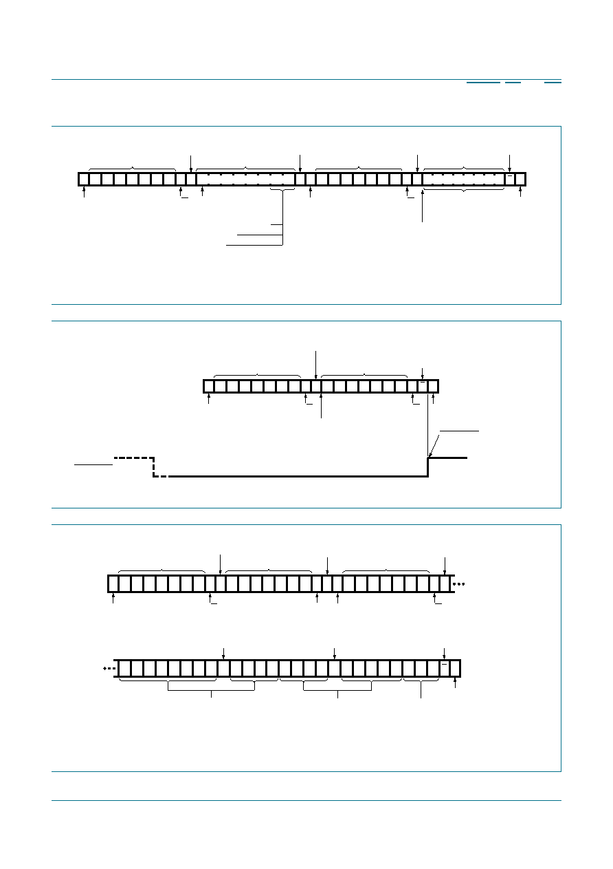
If AI = 0 or 1, the same register is read during the all sequence.
Fig 20. Read from output structure configuration, all bank control or mode selection registers
002aab949
S A6 A5 A4 A3 A2 A1 A0 0 A
slave address
R/W
START condition
command register
AI = 'don't care'
A
acknowledge
from slave
A
no acknowledge
from master
acknowledge
from slave
P
STOP
condition
SDA
X
01010 D1 D0
00 for output structure configuration register reading
01 for for all bank control register reading
10 for mode selection register reading
Sr
repeated START
condition
A6 A5 A4 A3 A2 A1 A0
slave address
1 A
R/W
acknowledge
from slave
data from register
DATA
last byte
At this moment master-transmitter
becomes master-receiver, and
slave-receiver becomes slave-transmitter.
Fig 21. SMBus Alert procedure
002aab950
A6 A5 A4 A3 A2 A1 A0 0
PCA9698 I2C-bus
slave address
R/W
A
no acknowledge
from master
P
STOP condition
S
0
1
0
SMBus Alert
response address
START condition
1 A
R/W
acknowledge from slave
that generated the alert
At this moment master-transmitter
becomes master-receiver and
slave receiver becomes slave-transmitter.
SMBALERT
SMBALERT signal is released
(assuming that only one device
generated the alert)
If more than 3 bytes are read, the slave device loops back to the first byte (manufacturer byte) and keeps sending data until the
master generates a ‘No Acknowledge’.
Fig 22. Device ID field reading
002aab951
A6 A5 A4 A3 A2 A1 A0
I2C-bus slave address
of the device to be identified
A
no acknowledge
from master
P
STOP condition
M
11
M
10
M9 M8 M7 M6 M5 M4
Sr
repeated START
condition
1 A
R/W
S
1
0
Device ID address
START condition
0 A
R/W
acknowledge from
one or several slaves
0 A
don't care
acknowledge from
slave to be identified
1
0
Device ID address
acknowledge from
slave to be identified
A M3 M2 M1 M0
acknowledge
from master
manufacturer name = 000000000000
P8 P7 P6 P5 A
acknowledge
from master
P4 P3 P2 P1 P0 R2 R1 R0
part identification = 000000000
revision = 000
发布紧急采购,3分钟左右您将得到回复。
相关PDF资料
ATMEGA328P-15AZ
MCU AVR 32K FLASH 15MHZ 32-TQFP
ATMEGA32L-8PJ
IC MCU AVR 32K 5V 8MHZ 40-DIP
ATMEGA32M1-AUR
IC MPU AVR 32K 20MHZ 32TQFP
ATMEGA48PA-MMNR
MCU AVR 4KB FLASH 20MHZ 28QFN
ATMEGA644P-B15MZ
IC MCU 8BIT 64KB FLASH 32VQFN
ATMEGA644V-10PU
IC AVR MCU FLASH 64K 40DIP
ATMEGA645V-8MI
IC AVR MCU FLASH 64K 1.8V 64QFN
ATMEGA649-16MI
IC AVR MCU FLASH 64K 5V 64QFN
相关代理商/技术参数
ATMEGA3250V-8AJ
制造商:ATMEL 制造商全称:ATMEL Corporation 功能描述:8-bit Microcontroller with In-System Programmable Flash
ATmega3250V-8AU
功能描述:8位微控制器 -MCU AVR 32K FLASH 1K EE 2K SRAM ADC 1.8V RoHS:否 制造商:Silicon Labs 核心:8051 处理器系列:C8051F39x 数据总线宽度:8 bit 最大时钟频率:50 MHz 程序存储器大小:16 KB 数据 RAM 大小:1 KB 片上 ADC:Yes 工作电源电压:1.8 V to 3.6 V 工作温度范围:- 40 C to + 105 C 封装 / 箱体:QFN-20 安装风格:SMD/SMT
ATMEGA3250V-8AUR
功能描述:8位微控制器 -MCU AVR 32KB FLSH 1KB EE 2KB SRAM-8MHZ 1.8V RoHS:否 制造商:Silicon Labs 核心:8051 处理器系列:C8051F39x 数据总线宽度:8 bit 最大时钟频率:50 MHz 程序存储器大小:16 KB 数据 RAM 大小:1 KB 片上 ADC:Yes 工作电源电压:1.8 V to 3.6 V 工作温度范围:- 40 C to + 105 C 封装 / 箱体:QFN-20 安装风格:SMD/SMT
ATmega325-16AI
功能描述:8位微控制器 -MCU AVR 32K FLASH 1K EE 2K SRAM ADC 5V 5V RoHS:否 制造商:Silicon Labs 核心:8051 处理器系列:C8051F39x 数据总线宽度:8 bit 最大时钟频率:50 MHz 程序存储器大小:16 KB 数据 RAM 大小:1 KB 片上 ADC:Yes 工作电源电压:1.8 V to 3.6 V 工作温度范围:- 40 C to + 105 C 封装 / 箱体:QFN-20 安装风格:SMD/SMT
ATMEGA325-16AJ
制造商:ATMEL 制造商全称:ATMEL Corporation 功能描述:8-bit Microcontroller with In-System Programmable Flash
ATmega325-16AU
功能描述:8位微控制器 -MCU 32kB Flash 1kB EEPROM 54 I/O Pins RoHS:否 制造商:Silicon Labs 核心:8051 处理器系列:C8051F39x 数据总线宽度:8 bit 最大时钟频率:50 MHz 程序存储器大小:16 KB 数据 RAM 大小:1 KB 片上 ADC:Yes 工作电源电压:1.8 V to 3.6 V 工作温度范围:- 40 C to + 105 C 封装 / 箱体:QFN-20 安装风格:SMD/SMT
ATMEGA325-16AUR
功能描述:8位微控制器 -MCU AVR 32K FLSH 1K EE2K SRAM ADC 5V-16MHZ 5V RoHS:否 制造商:Silicon Labs 核心:8051 处理器系列:C8051F39x 数据总线宽度:8 bit 最大时钟频率:50 MHz 程序存储器大小:16 KB 数据 RAM 大小:1 KB 片上 ADC:Yes 工作电源电压:1.8 V to 3.6 V 工作温度范围:- 40 C to + 105 C 封装 / 箱体:QFN-20 安装风格:SMD/SMT
ATmega325-16MI
功能描述:8位微控制器 -MCU AVR 32K FLASH 1K EE 2K SRAM ADC 5V 5V RoHS:否 制造商:Silicon Labs 核心:8051 处理器系列:C8051F39x 数据总线宽度:8 bit 最大时钟频率:50 MHz 程序存储器大小:16 KB 数据 RAM 大小:1 KB 片上 ADC:Yes 工作电源电压:1.8 V to 3.6 V 工作温度范围:- 40 C to + 105 C 封装 / 箱体:QFN-20 安装风格:SMD/SMT